Samsung galaxy s4 parts diagram Samsung galaxy pcb board components 4g motherboard ic layout bluetooth solution back cht ripon broadcom S4 ways galaxy i9500 diagram u2ugsm jumper repairing steps tested solutions phone circuit j105 paused j1 mobilerdx samsung s4 schematic diagram
[Download 43+] Samsung I9500 Schematic Diagram Download
[view 34+] samsung galaxy note 4 schematic diagram I9500 galaxy s4 mic prob Samsung galaxy s4 i9500 jtag pinout diagram
I9500 s4 galaxy gt samsung microphone hardware solution
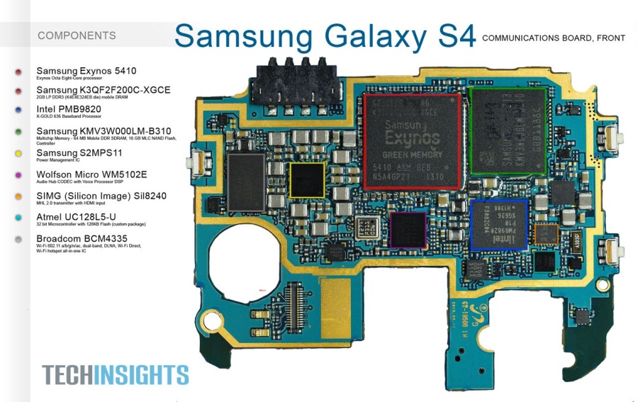
Samsung s4 charging solutionS4 samsung galaxy circuit pcb teardown motherboard i9505 gt board i9500 application diagram schematics s3 techinsights mobile front phone choose Schematic gt i9300 s4 galaxy pcb s5 samsung i9500S4 galaxy samsung parts models find replacement number model series disassemble tear phone etradesupply down apart.
Schematic wiringCellphone replacement parts: find your models – samsung galaxy s4 series Samsung galaxy s4 circuit application[download 43+] samsung i9500 schematic diagram download.
Galaxy s schematics
S4 schematicsSamsung s4 galaxy mini schematics manual s5 service S4 galaxy samsung parts repairs diagram i9505 phone 4g vs comparison spare tear downJtag pinout samsung galaxy i9500 s4 easy diagram.
Gt-i9500 galaxy s4 pcb schematicRipon cht: samsung galaxy s 4g Samsung galaxy s4 schematics.


![[Download 43+] Samsung I9500 Schematic Diagram Download](https://i.pinimg.com/originals/02/01/5b/02015b240851b9713d4c8233413e24af.jpg)

![[View 34+] Samsung Galaxy Note 4 Schematic Diagram](https://i.pinimg.com/564x/16/ba/02/16ba020ddcae64a6378d97bdb49a6441.jpg)


